

One of the most interesting announcements in Intel’s tidal wave of “Data-Centric” product and technology rollouts this month was the introduction of the company’s new “Agilex” FPGA families – formerly code-named “Falcon Mesa.” Agilex is the first new FPGA line developed by the former Altera group (now Intel PSG) since the Intel acquisition. Agilex is a milestone in the evolution of FPGA technology, and it brings substantial new capabilities to the party. It also represents a clearly divergent path from long-time archrival Xilinx, setting the stage for some interesting times ahead.
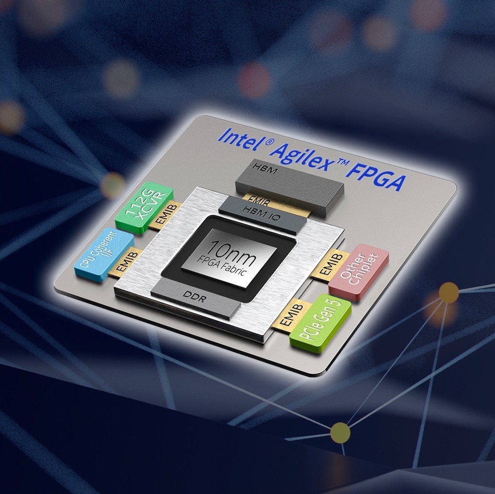
Agilex is cleverly built around Intel’s EMIB 2.5D packaging technology, which is an alternative to the interposer approach used in other “chiplet” ecosystems. The 10nm core FPGA LUT fabric is implemented as a chiplet and connected to other hardened features via EMIB. Agilex will also bring features like memory- and cache-coherency, with Xeon processors, 112 Gbps SerDes transceivers, support for PCIe gen 5, hardened support for BFLOAT16, and memory support for DDR5, HBM3, and Optane persistent memory.
Agilex will also welcome eASIC chiplets into the mix, allowing strategic hardening of critical functions that may have been initially implemented in FPGA fabric. This will allow design teams to deploy rapidly with FPGA-based designs and follow on with later cost-, performance-, and power-optimized eASIC blocks. The combination of a rich chiplet ecosystem and the EMIB technology allows Intel to raise the level of design abstraction for FPGA, and it brings the potential for design optimization and evolution not possible with monolithic FPGA designs.
The heterogeneous 2.5 approach Intel has chosen effectively conquers the “Swiss Army Knife syndrome” that plagues large FPGAs, where devices are crammed with hardened blocks that may be sparsely used by many designs. Countless variations of FPGA-in-packages can be created around a single set of FPGA fabric chiplets, and different hardened functions fabricated with completely different semiconductor processes can be mixed and matched. This will allow Intel and their customers to optimize FPGAs to a much greater degree without the need to spin new FPGA tape-outs or create myriad variations of monolithic FPGA chips.
The new FPGA fabric itself is implemented in Intel’s infamously late but impressive 10nm process technology, and it is built using an updated version of the “Hyperflex” architecture found in their Stratix-10 FPGAs, which peppers the fabric with storage elements that allow fine-grained pipelining and retiming of logic paths, greatly simplifying the challenge of timing closure in large, complex designs. Intel says the new devices can achieve either 40% better performance or 40% better power efficiency than Stratix 10, allowing designers to dial in their own compromise between performance and power efficiency gains.
The Agilex FPGA and SoC FPGA family brings “up to 2X the number of configurable multipliers per DSP block” compared to Stratix 10, targeting applications such as video, vision analytics, and radar. Intel is clearly aiming at accelerating AI workloads as well, with the introduction of hardened half-precision floating point (FP16) and BFLOAT 16, as well as low-precision configurations from INT8 down to INT2, claiming up to 92 TOPS INT8 performance. This range of precisions will allow inference models to be initially used as-is, facilitating later optimization via quantizing and moving to lower-precision, higher-performance inference.
The “SoC” versions of Agilex incorporate a full-featured quad-core Arm Cortex-A53 hard processor system that is backward-compatible with previous-generation Stratix 10 SoC FPGAs, facilitating software re-use. The A-53s operate at up to 1.5 GHz with 32 KB I/D cache, NEON coprocessor, 1 MB L2 cache, direct memory access (DMA), system memory management unit, cache coherency unit, hard memory controllers, two USB 2.0s, three 1G EMACs, two UARTs, four serial peripheral interfaces (SPI), five I2Cs, seven general purpose timers, and four watchdog timers. Agilex also includes a “Secure Data Manger” with AES-256/SHA-256 bitstream encryption/authentication, physically unclonable function (PUF), ECDSA 256/384 boot code authentication, and side channel attack protection.
Intel is boasting 112 Gbps PAM4 SerDes in Agilex, which piles onto their already-existing advantage with the only shipping 58 Gbps (which the company reportedly licensed from Broadcom and includes in chiplet form). The new 112 Gbps transceivers are said to be Intel-developed, however. The ability to mix and match transceivers from disparate processes highlights the flexibility EMIB gives Intel in quickly generating multiple variants of FPGAs-in-package without having to spin new silicon or have monolithic device development held up by the extreme challenge of new SerDes blocks on the same silicon with LUT fabric. Rival Xilinx’s currently-shipping devices max out at 28 Gpbs.
Intel is initially announcing Agilex in three flavors – F-series, I-series, and M-series. The F-Series FPGAs and SoC FPGAs target “a wide range of applications in Data Center, Networking, and Edge,” and it includes seven sizes ranging from 392K to 2.7M logic elements, from 38 to 259 Mb of M20K memory, and from 1,640 to 8,736 variable-precision DSP blocks, with a total of 2,300 to 17,056 18×19 multipliers. Apparently, Intel thinks we are gonna be doing a LOT of multiplication. Intel says these DSP resources give the F-series the capability to crank out 1.7/3.4 to 11.8/23.6 TFLOPS (depending on the device size) of single-precison/half-precision floating point performance. F-series supports DDR4, QDR IV, and RLDRAM 3 memory interfaces.
The interesting add-ons are done as chiplets (“tiles” in Intel parlance). The F-series includes “F-tile” resources such as PCIe hard IP blocks (Gen4 x16 ) or “bifurcateable” dual PCIe Gen4 x8 (EP) or quad Gen4 x4 (RP), 24-48 PAM4 transceivers operating at up to 57.8 Gbps, 32 or 64 NRZ transceivers operating at up to 32 Gbps, and four 10/25/50/100/200/400G Ethernet MAC + FEC hard blocks in larger devices. The F-series also includes “E-tile” and “P-tile” resources such as PCIe hard IP blocks (Gen4 x16 ) or bifurcateable 2X PCIe Gen4 x8 (EP) or 4X Gen4 x4 (RP), 12 PAM4 transceivers operating at up to 57.8 Gbps and 24 NRZ transceivers operating at up to 32 Gbps (in larger devices), and four 10/25/50/100/200/400G Ethernet MAC + FEC hard blocks in larger devices.
The I-Series SoC FPGAs are “optimized for high performance processor interface and bandwidth intensive applications” and come in two sizes – 2.2M or 2.7M logic elements with 6,250 or 8,736 DSP blocks (containing 12,500 or 17,056 18 x 19 multipliers). On-chip memory includes 210 Mb or 259Mb of M20K memory and 21 or 29.2 Mb MLAB memory.
The primary feature of note for the I-series is 48 lanes of “Compute Express Link (CXL),” which provide memory- and cache-coherent attachments to Intel Xeon processors. This gives Agilex a distinct advantage in co-processing with the ubiquitous Xeon processors in data center applications compared with (for example) Xilinx’s upcoming ACAP FPGAs (which are also targeting data center acceleration).
I-Series turns up the heat on the IO front as well, with substantial bandwidth courtesy of hardened PCIe Gen 5 support, 8x 112 Gbps PAM4 high-speed SerDes transceivers, 48x PAM4 58 Gbps transceivers, 8x 56 Gbps NRZ transceivers, and 64x 32 Gbps NRZ transceivers, as well as two hardened 10/25/50/100/200/400G Ethernet MAC + FEC blocks.
Less information has been released on the M-Series SoC FPGAs, which are “optimized for compute and memory intensive applications.” M-Series will also include Compute Express Line coherent attachment to Xeon processors, as well as HBM integration, hardened DDR5 controller, and Intel® Optane™ DC persistent memory support.
On the design tool front, Intel continues to evolve the Quartus design environment, claiming improved design-rule checking, “Fractal Synthesis,” which is supposed to improve performance for AI and DSP applications, a new/improved global router, and enhanced auto-pipelining to take advantage of the pipeline registers included in the Hyperflex architecture. At a higher level, Intel seems to be integrating and consolidating Quartus with a host of other development tools under their newly announced “One API” initiative.
The rollout of Agilex marks a notable inflection point and a fork in the road in the highly-competitive FPGA market, with Xilinx and Intel taking distinctively different approaches with both technology and marketing. The two companies may end up doing their selling to completely different audiences, as Intel is expected to bundle their FPGAs into numerous turnkey solutions such as complete servers and accelerator cards marketed by various OEMs. As a result, Intel’s biggest future FPGA customers may not be all that aware that they are even buying FPGAs. Xilinx, on the other hand, with their “Data center first” focus, is walking headlong into Intel’s turf – targeting big data center customers such as “Super 7” folks, who have the resources and wherewithal to design custom solutions around Xilinx’s devices. It will be interesting to watch the two strategies in action.


I don’t really see anything new except better marketing from Intel. It will still take hours to compile a design. They have done nothing about their randomized routing that messes up partial reconfiguration. They offer no tools to generate a bitstream in minutes (a totally doable task). Henry Ford once said “if I asked my customer what they wanted they would say a faster horse” This is a just faster horse.
@Beercandyman – I have to agree. They need a fast compile-load-and-go solution that hits 80% of best case SPEED in not more than 150% AREA, using functional tiles with easy partial reconfiguration of modules. Better speed and area optimization is something to do after you have a working solution.
It would be really nice to see the I-series chips closely coupled with Xeon’s soon … especially if Intel would give researchers (and open source developers) access to enough details about the low level architecture and bit stream to do place and route.
We did a pretty good job at proving C as an effective high-level synthesis language for compute projects 15 years ago, even in the face of some outright hostility for doing so. Now that industry has finally caught up, it would be really nice if Intel would let us finish, where Xilinx stopped us dead in our tracks asserting proprietary IP interests.