


The same year that I began my quest for a BSEE at Case Western Reserve University in 1971, someone posted a photocopy of a groundbreaking ad on the EE department’s bulletin board.
Here’s the ad:
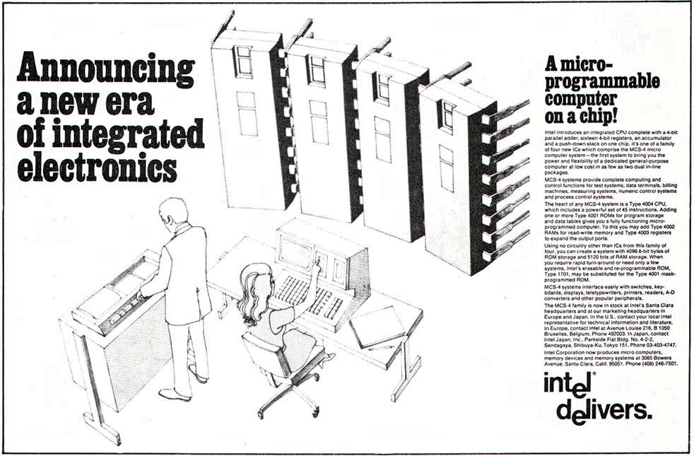
This ad appeared in the November 15, 1971 issue of Electronic News, which was the electronics industry’s publication of record at the time. (If you thought that would have been EE Times, you’re incorrect. The first issue of that newspaper appeared in 1972.) This ad announced the birth of Intel’s 4-bit 4004 microprocessor, the world’s first commercial microprocessor. With this ad, Intel served notice that it was about to turn the world upside down for design engineers and the electronics industry.
Prior to this ad’s appearance, digital design revolved around the development of logic circuits using heaps of SSI and MSI logic chips. By 1971, those logic chips were largely TTL devices. RTL and DTL logic chips preceded the TTL varieties by a year or two but were quickly superseded by the faster, more capable TTL varieties. Even so, TTL-based logic design was still just in its infancy in 1971 when Intel ran the ad for the 4004 Microprocessor.
TTL chips first appeared as SUHL (Sylvania Universal High-Level Logic) devices in 1963 and then snowballed when Texas Instruments introduced the ceramic-packaged SN5400 series in 1964, and then the reduced-cost, plastic-packaged SN7400 series in 1966. (Same semiconductor die, cheaper package.) National Semiconductor quickly became a second source for the TI TTL family. Then Motorola, Signetics, Sprague, and finally Fairchild followed suit (but only after TI co-opted many members of Fairchild’s 9300 logic family to grow its own 7400 series logic family).
According to the Computer History Museum’s TTL Web page titled “The Rise of TTL: How Fairchild Won a Battle But Lost the War,” TI remained the dominant and most profitable player in the TTL market with more than 50% of the worldwide market. That market reached annual sales of three quarters of a billion dollars by 1975.
Heavy duty TTL-based design was not even ten years old when the Intel 4004 was announced in 1971. Within another ten years, microprocessors would revolutionize and transform logic design from a hardware-design exercise into a largely software exercise. It all started half a century ago, today. The electronics world has never been the same since then.
It almost didn’t happen, Round 1
Fledgling Intel Corp was struggling in 1968. Robert Noyce and Gordon Moore founded Intel to develop and manufacture semiconductor memories: SRAMs and DRAMs. However, the memory chips were slow to reach production, and the company needed immediate revenue to survive in those early days, so Intel accepted custom IC design jobs as a way to help meet expenses.
Yes, Intel was in the foundry business back in the 1960s, more than 50 years ago. The recent creation of Intel Foundry Services is more of a return to Intel’s origins, rather than an all-new approach to chipmaking for the company.
One prospective customer, a Japanese calculator maker named the Business Computer Corporation (Busicom), had an elaborate plan for a large and complex chipset that it would use to build a modular desk calculator family. Busicom had already signed an agreement with Mostek to develop a custom calculator chip for a simple 4-banger calculator that would eventually be named the Busicom Junior. That calculator chip was the Mostek MK6010. It was one of several such chips to appear around that time, and possibly the first such chip. Single-chip calculator chips were the apex of LSI design in the late 1960s, and many chip vendors developed them.
However, Busicom also had bigger plans to develop a high-performance, programmable calculator. It would be called the 141-PF. Busicom’s Masatoshi Shima developed an elaborate, detailed, modular chipset for the 141-PF calculator. His design proposed twelve different LSI chips including a 3-chip CPU, ROMs that would add optional functions, a keyboard controller, a printer controller, and a display controller. Instead of binary, the chipset used decimal arithmetic for calculations, which was the basis for Busicom’s earlier mechanical calculators.
Shima presented his chipset proposal to Intel in 1969. It would require 3000 to 4000 transistors per chip, with 36 to 40 pins per package to implement the required interconnections among the twelve chips. Intel’s employee number twelve, Marcian “Ted” Hoff, evaluated the proposal and concluded that Intel could not develop or manufacture the chipset as Shima had designed it.
Intel was incapable of implementing Shima’s initial design for three reasons. First, Intel’s recently developed silicon-gate MOS process technology might cram 2000 or so transistors onto a chip, but Shima’s design would require twice that number. Second, because Intel was essentially a memory-chip company, the only IC packages it had on hand were narrow, 16- and 18-pin ceramic DIPs, far short of the pin count required in Shima’s design. Third, Intel had only two chip designers. They would not be able to design the required twelve chips in any reasonable length of time.
According to an article by Robert Noyce and Ted Hoff titled “A History of Microprocessor Development at Intel,” published in the premiere issue of IEEE Micro magazine in 1981, Hoff identified three significant sources of complexity in Shima’s design that hindered implementation using the resources available to Intel at the time:
- Most of the peripheral control logic needed to operate the calculator’s keyboard, display, and printer was implemented using separate chips, which ballooned the required number of transistors and the chip count.
- The proposed shift register memory (very common in electronic calculators of the day) required fairly complex timing. Hoff thought Intel could simplify the memory design using DRAM.
- The proposed decimal CPU instructions were quite intricate. Many required one or more data passes through a register to alter both the mantissa and the exponent of a floating-point number. Even though some of the proposed CPU logic had been implemented with ROM in Shima’s design, a major portion still required random logic circuits.
Hoff was familiar with Digital Equipment Corp’s PDP-8 minicomputer. He realized that he could reduce the logic complexity in Shima’s design by shifting more of the calculations to software running on a more general-purpose, binary CPU. However, a single-chip version of the 12-bit PDP-8 minicomputer architecture was equally beyond Intel’s integration capabilities in 1969. Hoff knew the design problem’s solution would demand something even simpler. (Note: Intersil did fit a PDP-8 CPU on one chip in 1975 – the Intersil 6100 – using 4000 transistors.)
In their IEEE Micro article, Noyce and Hoff wrote:
“A four-bit data quantity seemed natural for BCD arithmetic. With four-bit binary and separate instructions to convert the result back to BCD, addressing of up to 16 digit positions could be retained. Members of the calculator family would vary both in function and the number of registers required. To meet this need for flexibility, the Intel team decided on a three-chip design: a CPU, a ROM for program memory, and a RAM for data memory.” [Shima subsequently added an I/O expander chip to the chipset.]
Intel’s analysis of Hoff’s proposed processor architecture indicated the design would meet the needs of Busicom’s planned 141-PF calculator family. The next question that Intel needed to answer was whether the company could manufacture this chipset in a cost-effective manner. Les Vadasz, head of Intel’s MOS design team, worked with Hoff and Stan Mazor to develop chip-size estimates. The team initially estimated that the chips would need about 1900 transistors each, which was within Intel’s manufacturing capabilities at the time. (In final form, the Intel 4004 CPU needed more than 2100 transistors.)
Ultimately, the 4-chip set would be called the MCS-4. It consisted of:
- The 4001, a 256-byte ROM
- The 4002, a 320-bit RAM capable of storing four 20-digit numbers
- The 4003, a 10-bit I/O Expander (essentially a shift register used to transform the 4004 CPU’s complex, multiplexed bus into a parallel I/O port)
- The 4004, a 4-bit CPU
Each of the four devices would be packaged in a 16-pin ceramic DIP. To reduce pin count, the MCS-4 chipset employed a relatively sophisticated, multiplexed bus protocol that transferred addresses and CPU instructions between the MCS-4 chips over a 4-bit bus using multiple clock cycles. For example, an instruction fetch required five clock cycles: three cycles to transfer the 12-bit address from the CPU and two cycles to retrieve the 8-bit instruction from memory. There weren’t enough pins available to have separate address and data buses.
Each chip in the MCS-4 chipset needed to incorporate logic to handle this bus protocol. That logic included timing and control circuits, an address register, and a data register for an integrated I/O port in each chip. The MCS-4 RAM and ROM chips also incorporated integrated I/O ports to reduce the number of chips needed to build a system, so these chips monitored the system bus, recognized and decoded I/O instructions, and responded accordingly. That meant the CPU didn’t need to run explicit I/O cycles. This sort of distributed instruction decoding capability is unusual and underscores that the MCS-4 was a purpose-designed, integrated chipset developed for embedded designs and not just a collection of general-purpose computer chips.
Meanwhile, Busicom’s design team worked to simplify Shima’s original calculator chipset design, but even the simplified version still required twelve chips. Although the revised design now averaged a little more than 2000 transistors per chip, each chip in the design still needed 36 to 40 pins.
Shima visited Intel along with Busicom executives in September or October of 1969 to make the final choice between the two designs. Shima saw promise in Hoff’s proposal but was not overly impressed with it because the proposal consisted of a very high level architectural description and lacked implementation details. Despite its radically different, software-centric architecture, Busicom’s execs eventually approved Hoff’s design proposal on October 21, 1969 because it appeared to offer a less costly solution. Busicom agreed to pay Intel a large development fee to create the proprietary chipset needed to build the 141-PF calculator.
Shima returned to Japan and spent the next several months developing ideas for the calculator, writing several preliminary firmware programs using the proposed instruction set, and using the results of that work to refine the CPU’s instruction set. Meanwhile, Intel made no progress on the MCS-4 chipset design.
Stay tuned for Part 2 of this article to find out why.
References:
Note: Because the Intel 4004 plays such a huge role in semiconductor history, its origins have been the subject of many, many articles over the past 50 years. Some of the information in these articles is accurate. Some appears to be less than accurate. This article is based on primary references written by the principals involved in the project and on oral histories as told by the principals. It’s also based on the Robert Noyce biography written by noted Silicon Valley historian, author, and Project Historian for the Silicon Valley Archives at Stanford University, Dr. Leslie Berlin. In my opinion, that’s the most accurate way to tell this story.
N. Noyce and M. E. Hoff, “A History of Microprocessor Development at Intel,” in IEEE Micro, vol. 1, no. 1, pp. 8-21, Feb. 1981, doi: 10.1109/MM.1981.290812.
Masatoshi Shima, an oral history conducted in 1994 by William Aspray, IEEE History Center, Piscataway, NJ, USA. https://ethw.org/Oral-History:Masatoshi_Shima#Tedd_Hoff.27s_Initial_LSI_Design
Intel 4004 microprocessor oral history panel, Computer History Museum, April 25, 2007. https://www.computerhistory.org/collections/catalog/102658187
Berlin, Leslie. The Man Behind the Microchip: Robert Noyce and the Invention of Silicon Valley. Oxford: Oxford University Press, 2005.


Hi Steve — I’ve read a lot about the 4004 (I have one of the original ceramic packaged devices in my little collection) — most of it was reasonably accurate but some of the details got a little fluffy around the edges — so I’m really enjoying reading your “from the horse’s mouth” articles — Max
Neigh, Max. I didn’t have hands-on experience with the 4004. Just a bunch of other microprocessors that followed.